For 2019 I had a goal of designing my first PCB, and this week I accomplished that goal. The idea of designing a PCB was pretty intimidating so I decided to try and design the simplest possible PCB I could. For me, this translated to “a board with a single, GIANT LED”. I named this board ‘Spot’.
Prior to this project I had gotten some experience and enjoyment out of interacting with GreatFET while designing my robot hardhat Shellie, so I decided that the PCB I wanted to design should be a neighbour for GreatFET. Thankfully, Michael Ossmann was available and willing to mentor me through the creation of this PCB.
Designing the PCB took about three hours of learning and work, but it was definitely worth the effort. The steps I took were as follows.
Step 1: Find the biggest LED.
Since the LED was the focal point (and only point) of the PCB, I wanted to make sure I could find the right LED that would make me feel like this project was a success. The first (and coincidentally last) place I decided to look was on Digi-Key. Once I was on the site, the next step was to look for LEDs. At this point I found out that there were more types of LEDs than I was expecting. After some poking around in the categories it was apparent that what I wanted was in the “LED Indication — Discrete” category.
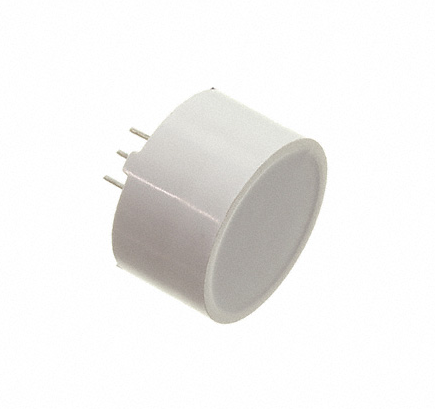
Next I needed to whittle down my options. I chose to filter the results by whether the item was in stock, and then I sorted the LEDs by size with the biggest ones shown first. I was delighted to see a “chonky” multi-colour LED (product number 4042) by Adafruit was at the top of the list. I initially chose this LED for its size, but I also liked it because it wasn’t blindingly bright, it was multi-colour, and I liked the look of the flat top. Picture of the LED that I chose for this project (Adafruit 4042).
Step 2: Look up how to create a GreatFET neighbour.
The best way to figure out how to make a GreatFET neighbour was to Google “how to make a GreatFET neighbour”. The query brought up the following website: https://greatfet.readthedocs.io/en/latest/design_neighbor.html. Next, I followed the instructions on the website to get started with the GreatFET neighbour template in KiCAD.
(I already had KiCAD installed before starting this project.)
Step 3: Start designing the GreatFET neighbour.
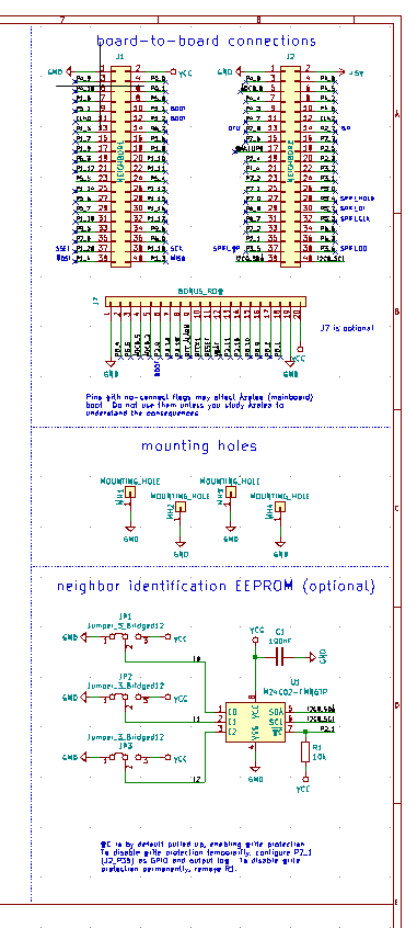
I quickly learned that there were two major steps to designing a PCB: the schematic entry phase and the PCB layout phase. To start designing my schematic for the PCB I clicked on the ‘schematic layout editor’ button at the top of the screen and reviewed what came up. Since I was working from the GreatFET neighbour template, the schematic already had a number of pre-designed components visible: the board-to-board connectors, the mounting holes, and the neighbour identification EEPROM. The big blank area to the left on the schematic is where I designed the rest of my board. GreatFET neighbour template pre-designed components.
At this point I realized I had no idea what to place on the schematic and why.
Step 4: Learn about the LED that was chosen.
To learn about the LED that I chose for this project and how to represent it on a schematic, I headed back to Digi-Key to read the data sheets that they had available for the part. I was able to find out some important technical details such as forward voltage for the two LEDs that were encased in the single giant LED package and that the center pin of the three pins on the package was a common cathode. The two LEDs encased in the package were red and green. Additionally I learned that I would need to place a resistor in series between the power supply and each of the outer LED pins. Yet, I still felt I was missing information after reading the documentation. For example, how far apart were the pins?, which outer pin controlled what colour?, and so on, so I headed to the Adafruit website for the LED to learn more.
On the Adafruit website, I watched the product video for the LED and was able to figure out that the pins were probably .1" apart. I did not find out which outer pin was for which colour LED, but I decided I would figure that out when I build my prototype.
Step 5: Continue designing the board in KiCAD.
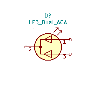
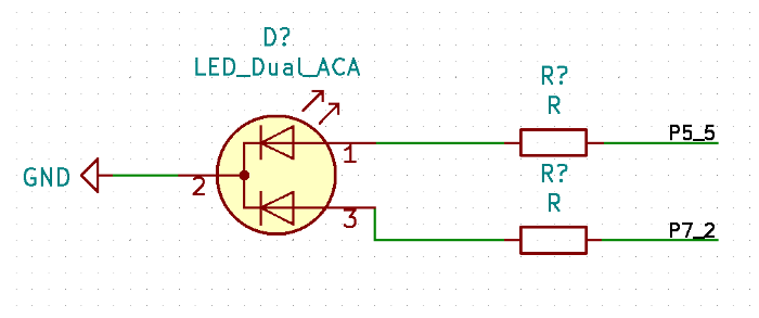
Now that I knew that the LED had three pins and the middle one was a common cathode I could pick the right schematic symbol to place in my design. To place the LED symbol on the schematic I pressed the ‘a’ button, moved to the LED section in the window that popped up, and slowly started looking through all of the possible parts. It took a bit of searching and term lookup but eventually I was able to find ‘LED_Dual_ACA’. I placed the part on the schematic by selecting the part, clicking ‘OK’ and clicking on the schematic screen. LED schematic symbol chosen for this project.
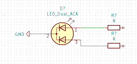
Next, I placed the two resistors needed between each LED and the power supply onto the schematic. It is then that I learned that the most common schematic symbols in KiCAD generally have the shortest names. For example, a resistor is ‘R’. After the resistors, I placed the ground symbol, which in KiCAD is ‘GND’. At this point all the required parts were on the schematic and all I had to do was connect them.
To place wires I pressed ‘w’, clicked where I wanted the wire to start and double clicked where I wanted the wire to end. I connected ground to the middle pin, one outer LED pin to one of the resistors, and the other outer LED pin to the other resistor. Placing wires did not work how I expected based on my previous experience with graphing software, so I had to put a lot of effort into training myself out of my keyboard muscle memory for similar tasks. Schematic with all components connected.
At this point my schematic still did not have a way power to the LEDs or a way to control them.
Step 6: Choose the GPIO pins to control and power the LED.
Providing power to LEDs and controlling them can be done through GPIO pins, so my next step was to choose a couple of GPIO pins to connect my LED to. As mentioned in Step 3, the ‘schematic layout editor’ was already displaying the board-to-board connections for GreatFET neighbours, so I could choose two of those to power and control my LED.
Many of the pins were already labelled, so I avoided those. At this point I was also told by Michael Ossmann to look at the GreatFET sticker and avoid the pins that were labelled there as many of them have a dedicated purpose. It was then that I learned about https://github.com/greatscottgadgets/greatfet-pinout which provides pin details, such as which pins may be used for GPIO functions. In the end I chose pin 23 on one header, and pin 23 on the other header.
Next, I went back to my schematic and detailed which GPIO pin connected to which resistor. To connect the GPIO pins to the resistors, I drew wires out from both of the resistors and terminated them a little bit out from the resistor. I then copied the label from pin 23 from one of the headers and affixed that to the end of the wire from one resistor, and then repeated this process for the other wire using the other pin 23 from the other header. Schematic with all components connected and the resistors connected to the GPIO pins.
Step 7: Math
LEDs violate Ohm’s Law; they will run away with current and they will pop. To protect my LEDs I needed to find the right resistor value to place between the power supply and the LEDs. Thankfully, resistors follow Ohm’s law, so I could figure out the value of resistor I needed by calculating V = IR, or in this case R= V/I.
To find ‘V’ I had to find out how much voltage was supplied by GreatFET and what the forward voltage of the LED was. I found out from the ‘How to design a neighbour’ page that “Except for +5V, all pins on the neighbor interface are referenced to 3.3 V”. On the Adafruit webpage I found out that each of the LEDs in the giant LED package each had “about 2.3V forward voltage”. Looking back at the Digi-Key documentation though, one of the LEDs had 2.1V forward voltage so I designed for that LED instead. To calculate ‘V’ I subtracted the LED voltage from the GreatFET voltage to get: 3.3V-2.1V=1.2V.
To find ‘I’ I went back to look at the LED product documentation and found out that it could handle a 25 milliamp current. I chose a 15 milliamp current instead because I wanted to stay well away from the maximum current for the LED. Then, to find what the value of the resistor should be I calculated R = V/I = 1.2V/.015A = 80 Ohms. At this point I looked back at the Adafruit video to see what resistors they used with the LED, and it turns out they used 100 Ohm resistors. That’s close enough to 80 Ohm resistors so I followed what Adafruit did and went with 100 Ohm resistors.
Step 8: Add information to the schematic.
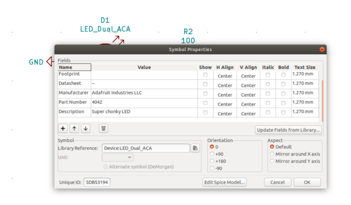
Next I labelled and added information to the schematic to make sure that others (including future me) would be able to decipher my intentions. To add information to each component I hovered over each part one at a time and pressed ‘e’. In the screen that popped up I added a link to the datasheet for the part I selected, and then added new fields so I could list the manufacturer, part number, and a description for the part. Adding extra information to the LED component.
Step 9: Choose component footprints.
The last bit of information I needed to add to my schematic was the footprint for each component. I started assigning footprints to components by selecting a suitable footprint for the resistors. I was able to reduce my resistor footprint options to one I liked by ignoring ‘vertical’ resistors. Then I measured a resistor that I had soldered onto another board in a previous project to determine what length resistor I wanted to use. The footprint I ended up choosing was ‘Axial_DIN0207_L6.3mm_D2.5mm_P10.16mm_Horizontal’, which is a really long way to say a resistor with pins about 10mm apart.
The only other part I needed to find a footprint for was my LED, and I was concerned that I wouldn’t find any suitable options. Luckily, KiCAD had a footprint ‘LED_D10.0mm-3’ which was a three pin, two LED package. The only problem with this footprint was that it was 10.0mm in diameter and not 18.0mm in diameter like the LED I found. Thankfully, the pins were the correct distance apart and the footprint was fine otherwise. I decided that I could deal with this in the ‘PCB layout’ phase of this project.
At this point the schematic design phase was complete, and so was the first major step to building a PCB.
Step 10: Board layout.
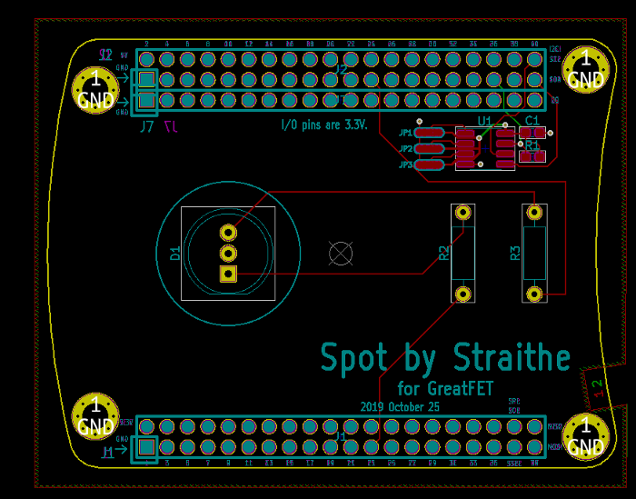
This step was surprisingly easy because much of the PCB layout was already in place via the GreatFET neighbour template. The only layout work I had to worry about was placing the LED, the two resistors, updating the silk screen, and routing.
For design purposes I wanted the LED front and center, so I placed it about a third from the left of the board. I then drew an 18.0mm circle on the silkscreen that was centered on the middle of the LED footprint so I could accurately see how much room the LED was going to take up on the neighbour.
Following the placement of the LED, I placed the two resistors on the right side of the board to balance out the LED on the left. I lined the rightmost LED up with the edge of the GreatFET neighbour headers. Routing was fairly simple as I only had to click where I wanted the trace to start and where I wanted it to end. Then, to update the silk screen I pressed ‘e’ overtop of the existing neighbour text and updated what was there to reflect myself and my project. Finished PCB layout design.
With that, my board was done!